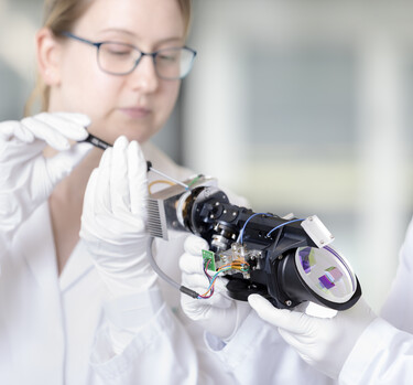
Coatings & Microstructures. Application-Specific Surfaces.
We produce superior coatings for various applications. The spectral range runs from UV (190 nm) into the infrared range (5 µm; up to 12 µm for metal mirrors).
With our modern coating technologies (PVD with and without ion-assistance), we have extensive coating capacity with in-situ monitoring technologies (oscillating quartz and optical broadband monitoring) in order to provide you with specific solutions. The most modern measurement and testing techniques allow us to analyze even very demanding specifications.
Our coating services include
- Coatings on typical optical glass as well as quartz, sapphire, CaFl2, Si, Ge, ZnS
- Formats from diameters of 3 mm upwards, planar components up to 400 mm in length
- Also, glass fibers, cemented substrates, crystals
- Spectral range of 190 – 5,000 nm, mirrors from 190 nm – 12 µm
- Conductive coatings (ITO), anti-glare absorption layers (e. g. black chrome, chrome-free as well)
- High laser damage thresholds (LIDT)
- Strict coating tolerances
- ROHS compliant
In addition, we design and manufacture micro-structured optical components according to your wishes.
Through the use of various lithographic processes (lift off, etching processes, contact prints, proximity copies, imaging copies), we are able to find the perfect solution for optical masks, apertures, reticles and calibration plates.
More information on our coating development services is available under
Areas of application
Our products are currently used in the following fields
- Apertures for endoscopes and other optical devices
- Measuring solids in measurement and testing techniques
- Reticles with crosshairs and similar structures used in telescopic sights or for optical measurement and analysis devices
- Optical calibration standards for measurement machines with optical scanning
- Resolution tests for microscopes and lenses
Specifications
| Substrate types | Optical glass, colored glass, quartz, sapphire, semiconductor materials, glass fibers, crystals (laser resonators) |
|---|---|
| Spectral range | AR: 190 to 5,000 nm, mirrors: 190 to 12,000 nm |
| Structuring | Up to 1 μm possible with an accuracy of 0.2 μm depending on the structure design |
Metrology / QS
- Various spectrophotometers for reflection & transmission (190-3,000 nm), optical density and polarization
- Environmental/climate tests according to ISO and MIL (heat, moisture, autoclaving)
- Abrasion and adhesive tests
- Surface measurement technology (tensiometers)
- Various tests with regards to chemical resistance
- 4-point resistance measurement technology for conductive layers
Antireflective layers (AR)
Poorly reflective coatings of 190 nm to 6 µm
- AR broadband (Rabs 400-1,100 nm < 1 %)
- AR with low reflectivity (Rabs @ λ < 0.1 %)
- Laser damage resistant coatings (pw & cw applications)
- Multi-incidence angles (0-45° typical, 0-85° possible)
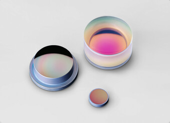
Antireflection coatings
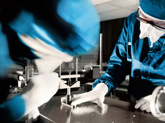
Transmission testing of 193 nm
Filter layers
- Single band filter/laser protection filter
- Multi band filters
- Edge filters
- Line filters
- Narrow band filters
- Graduated filters
Polarizing and non-polarizing beam splitting coatings
- Chromatic beam splitters
- Intensity beam splitters
- Polarizing and non-polarizing beam splitters > TS/TP extinction ratio up 1000/1
- Cemented beam splitters and beam splitters with defined air gap cementing
Mirror coatings
Highly reflecting metallic and dichroitic mirror coatings 120 nm to 12 µm
- Boosted dielectric and metallic mirrors
- Broadband mirrors (Rabs 400-1,000 nm > 98 %)
- High reflectivities (Rabs @ λ > 99.5 %)
- Multi-incidence angle (0-45° typical, 0-60° possible)
- Mirror coatings for laser applications (20 J/cm2)
- Front and rear surface mirrors
- Stress-optimized coating designs
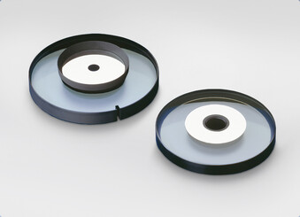
Formed lenses with metal mirrors
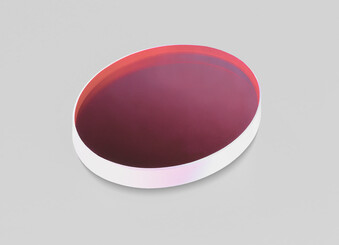
Dichroitic mirror coating
Absorption layers (LRC/HRC)
- Absorption layers with low reflection (black chrome)
- High optical densities up to OD7
- Narrow and broadband coatings
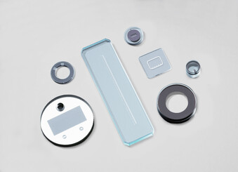
Microstructured chrome coatings
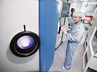
APS system
Transparent and electrically conductive layers (ITO)
Manufacturing of conductive (adjustable resistance) ITO coatings, however highly transparent in the visible range (e. g. to heat front surfaces for optical systems susceptible to condensation, or as transparent electrodes)
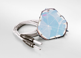
Retroreflector with ITO coating
Microstructures
Lithographically structured, arbitrary coatings in the µm range allow for new applications in high-end imaging opto-electronic systems with simultaneous, specific spectral sensitivities.
- Tessellation and line filters
- Filters with various structured geometries
- Color-coded systems (not just black and white)
- Colored reticles
- Colored gradient filters
- Color filters
For additional technical details about the options for microstructuring, please see the data sheet
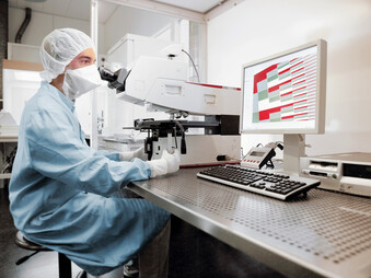
Testing for a structured coating
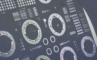
Microstructured coatings

Microstructured chrome coatings
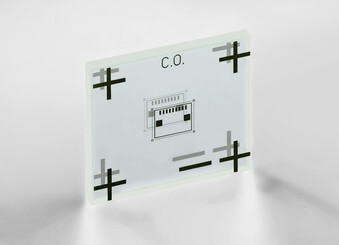
Optical calibration standards
Finishing techniques
- Plug/screen printing
- Edge/spray painting
- Optically dense finishes
Contact our specialists
Please choose your contact partner:





Let us call you back!
SwissOptic AG
Heinrich-Wild-Strasse
9435 Heerbrugg, Switzerland
Phone +41 71 747-0420
swissoptic@swissoptic.com


